Confocal Raman Microscopy
A Brief Overview of Raman Spectroscopy
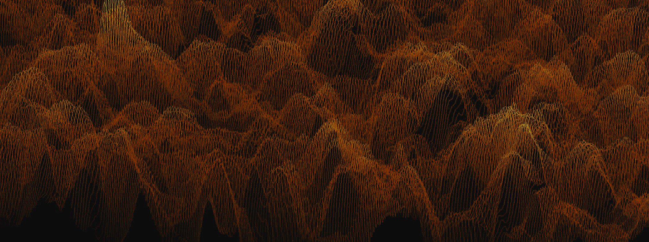
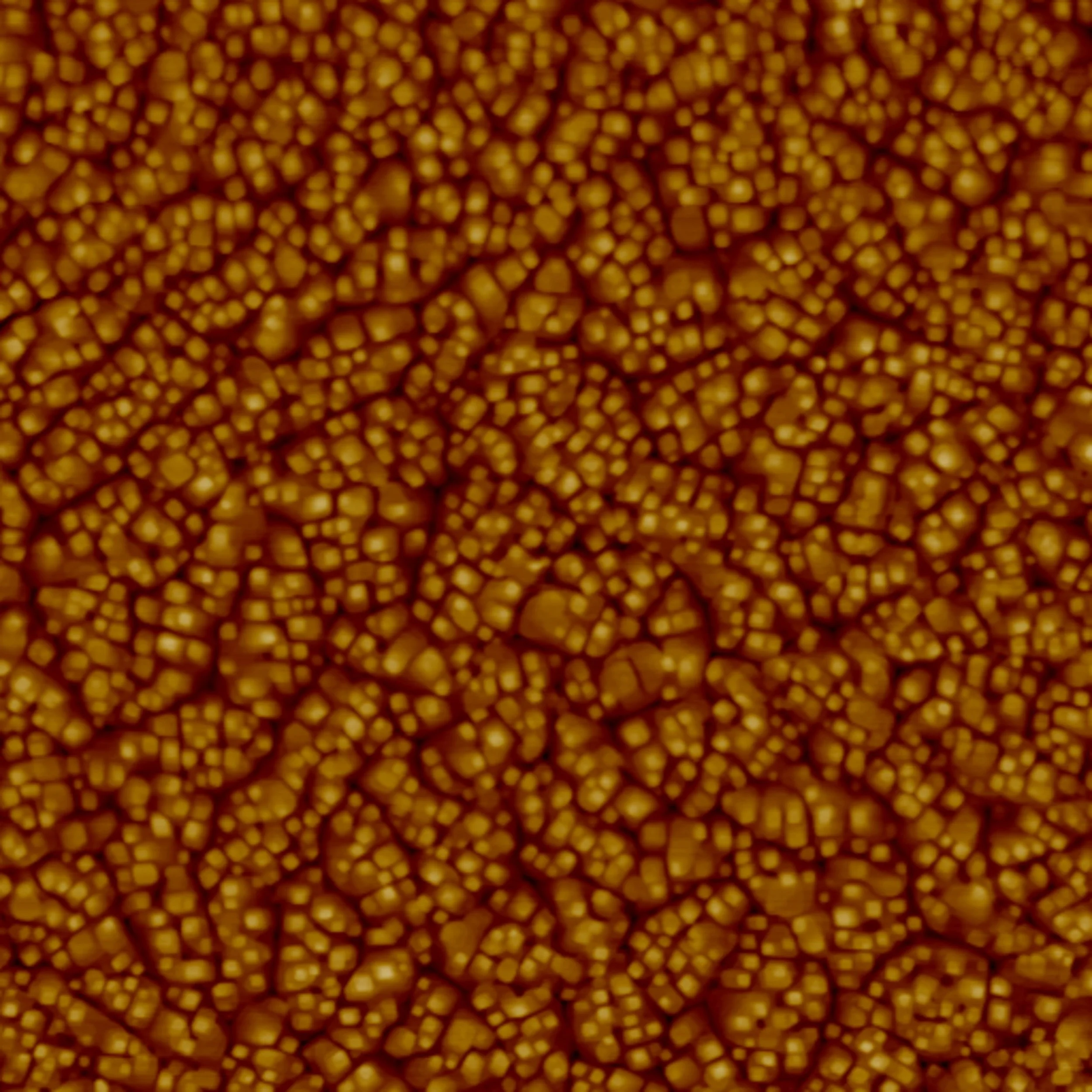
Atomic force microscopy (AFM) is a scanning probe microscopy technique that uses a sharp tip to image a sample. Inspired by developments in stylus profilometry the first AFM was developed in the 1980s by Gerd Binnig, Calvin Quate, and Christoph Gerber. This type of microscopy was (and remains) revolutionary as it now enables atomic resolution without the expensive high-vacuum systems and complicated optics required by high-resolution electron and optical microscopes. AFM can image almost any type of sample, enables collection of three dimensional datasets and can be modified to simultaneously collect electrical, magnetic, mechanical, chemical, and topographic data. AFM has been used for everything from identifying individual atoms in semiconductor films to imaging individual macromolecules in biological cells to building and manipulating nanostructures. In thin film research AFM is often combined with electrical and spectroscopic measurements to study and improve a wide range of materials and devices. For more information about the incredible versatility and scope of this technique we recommend the textbook Atomic Force Microscopy by Peter Eaton and Paul West and the extensive webinar series and application notes available from the manufacturer of our instrument - Bruker.
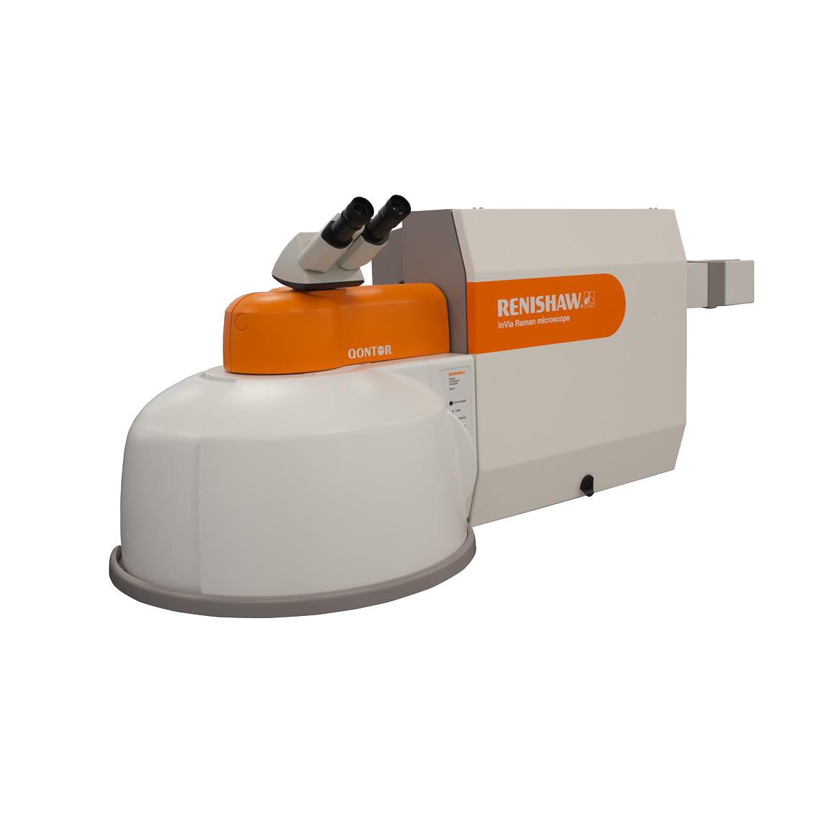
About Our Instrument
The Renishaw inVia Qontor and Linkam THMS600
Raman is among the most widely used techniques in the LRG’s research. We use Raman to study material distribution, purity, nanoscale self-assembly, temperature responsiveness, analyte sensitivity, and more. The ability to evaluate both liquid and solid samples quickly, easily, and reliably makes this one of most widely used instruments that receives dedicated support from several skilled operators.
Extensive Imaging Options
Our system has four lasers at 405, 532, 785, and 830 nm that allow us to image a wide range of materials. Equipped with an internal reference standard and housed in a Class 1 laser system the inVia provides rapid and reliable analysis. We regularly use the mapping capabilities of this microscope to study material composition over a range of small and large areas using Renishaw’s LiveTrack capabilities and the full selection of objectives in the embedded Leica Microsystems microscope. For specialized experiments we open the enclosure and use our Linkam THMS600 stage to perform Raman analysis while exploring a wide range of experimental conditions ranging from active electrical operation to atmospheric control to thermal analysis over a range extending from cryogenic temperatures up to 600 °C.

System Specs
Vertical Resolution: ~ 1 nm
Features Resolution: ~ 2 nm (depending on probe and scan size)
Scan Area:
Icon: Up to 80 x 80 um
FastScan: Up to 30 x 30 um
Typical Runtime per Sample:
Icon: 10 minutes per scan (standard imaging)
FastScan: 5 minutes per scan (standard imaging)
Running Samples with the LRG
Samples should be provided on a flat substrate (typically a silicon wafer or glass slide). Samples that require special mounting may take longer to prepare and are usually affixed to small metal disks using adhesives which are then magnetically mounted on the microscope stage.
We typically require confirmation that a sample is well below the vertical limit of the scanhead being used before we start imaging (4 um for the FastScan and 12 um for the Icon). For features larger than 2 microns in height we recommend using our 2D stylus profilometer or optical microscope.
Some experiments may require a specific scanhead and may require changing the instrument configuration. We also have a wide range of probes that can be selected based on the experimental requirements. If you have any insight into your sample modulus or any restrictions related to subsequent analysis or sample integrity please contact us to discuss our options for low-spring constant probes, fine-tip resolution probes, and non-destructive imaging options.
Raman in Research
-
![]()
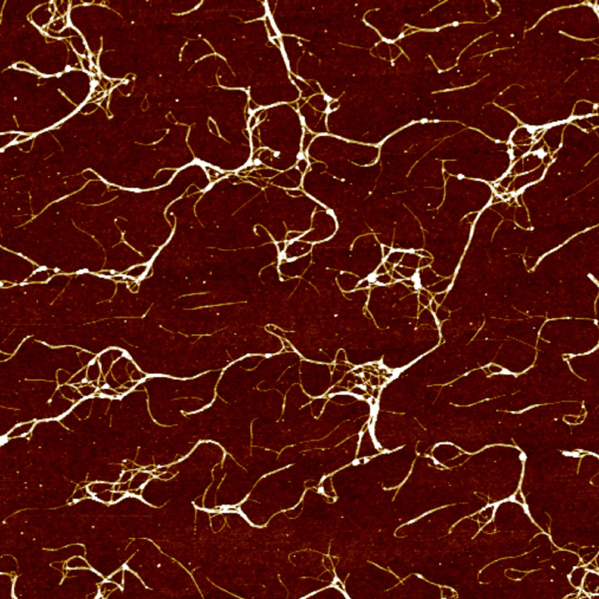
At the Nanoscale
Bundles of nanotubes
-
![]()
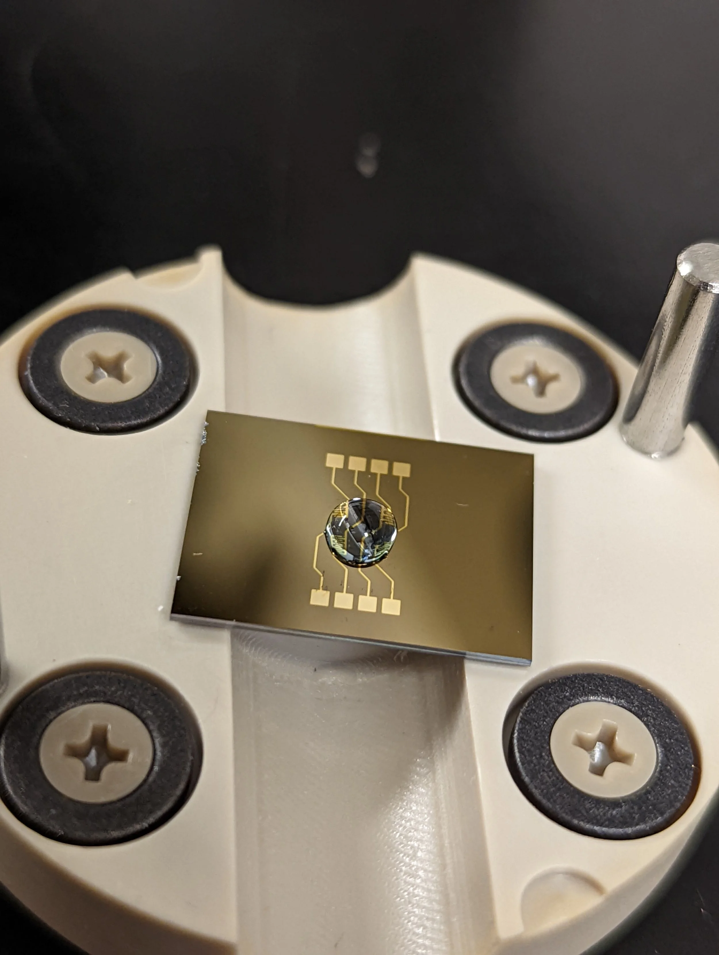
It's a Title
More example text briefly discussing the work and also linking to a paper
-
![]()
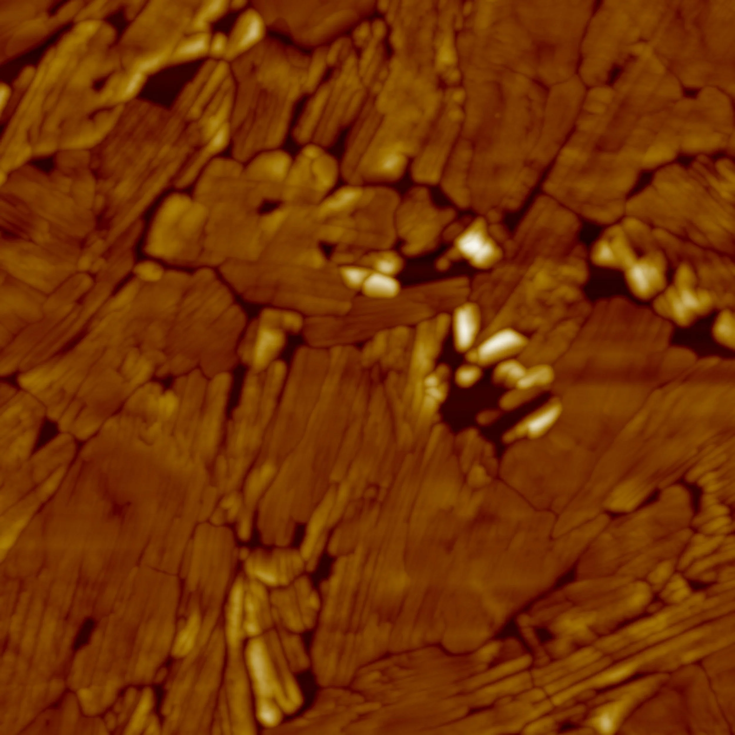
Siloxane SiPc
Annealing makes all the difference. Our AFM captures nanoscale assembly changes in these siloxane SiPcs. Read more in ~linked article~
References
List of references